- 您现在的位置:买卖IC网 > Sheet目录364 > SST39VF3201B-70-4I-EKE (Microchip Technology)IC FLASH MPF 32MBIT 70NS 48TSOP
32 Mbit Multi-Purpose Flash Plus
SST39VF3201B / SST39VF3202B
Data Sheet
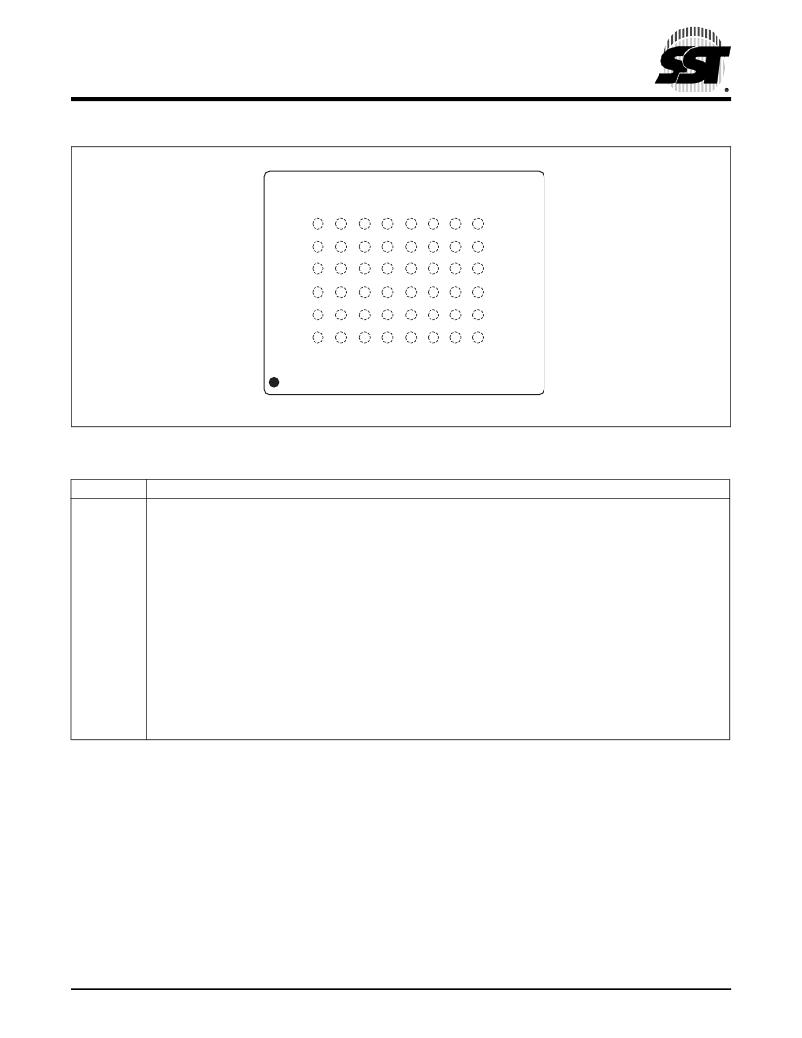
TOP VIEW (balls facing down)
6
A13 A12 A14
A15 A16 NC DQ15 VSS
5
A9
A8
A10
A11 DQ7 DQ14 DQ13 DQ6
4
WE# RST#
NC
A19 DQ5 DQ12 VDD DQ4
3
NC WP# A18
A20 DQ2 DQ10 DQ11 DQ3
2
1
A7
A3
A17
A4
A6
A2
A5
A1
DQ0 DQ8 DQ9 DQ1
A0 CE# OE# VSS
A B C D E F G H
1384 4-tfbga B1K P2.0
FIGURE 3: pin assignments for 48-ball TFBGA
TABLE 4: Pin Description
Symbol
A MS1 -A 0
DQ 15 -DQ 0
WP#
RST#
CE#
OE#
WE#
V DD
V SS
NC
Pin Name
Address Inputs
Data Input/output
Write Protect
Reset
Chip Enable
Output Enable
Write Enable
Power Supply
Ground
No Connection
Functions
To provide memory addresses.
During Sector-Erase A MS -A 11 address lines will select the sector.
During Block-Erase A MS -A 15 address lines will select the block.
To output data during Read cycles and receive input data during Write cycles.
Data is internally latched during a Write cycle.
The outputs are in tri-state when OE# or CE# is high.
To protect the top/bottom boot block from Erase/Program operation when grounded.
To reset and return the device to Read mode.
To activate the device when CE# is low.
To gate the data output buffers.
To control the Write operations.
To provide power supply voltage: 2.7-3.6V
Unconnected pins.
T4.0 1384
1. A MS = Most significant address
A MS = A 20 for SST39VF320xB
?2009 Silicon Storage Technology, Inc.
7
S71384-01-000
1/09
发布紧急采购,3分钟左右您将得到回复。
相关PDF资料
SST39VF3202C-70-4I-EKE-T
IC FLASH MPF+ 32MBIT 48-TSOP
SST39VF512-70-4I-NHE-T
IC MEM MPF 512MBIT FLASH 32PLCC
SST39VF6401B-70-4I-B1KE
IC FLASH MPF 64MBIT 70NS 48TFBGA
SST39WF1602-70-4I-MBQE
IC FLASH MPF 16MBIT 70NS 48WFBGA
SST39WF400A-90-4I-ZKE
IC FLASH MPF 4MBIT 90NS 48CSP
SST39WF400B-70-4I-MAQE-T
IC FLASH MPF 4MBIT 70NS 48WFBGA
SST39WF800B-70-4C-EKE
IC FLASH MPF 8MBIT 70NS 48TSOP
SST49LF008A-33-4C-EIE-T
IC FLASH FWH 8MBIT 33MHZ 40TSOP
相关代理商/技术参数
SST39VF3201B-70-4I-EKE-T
功能描述:闪存 2.7 to 3.6V 32Mbit Multi-Purpose 闪存 RoHS:否 制造商:ON Semiconductor 数据总线宽度:1 bit 存储类型:Flash 存储容量:2 MB 结构:256 K x 8 定时类型: 接口类型:SPI 访问时间: 电源电压-最大:3.6 V 电源电压-最小:2.3 V 最大工作电流:15 mA 工作温度:- 40 C to + 85 C 安装风格:SMD/SMT 封装 / 箱体: 封装:Reel
SST39VF3201C-70-4I-B3KE
功能描述:闪存 2.7V to 3.6V 32Mbit Multi-Prps Fl RoHS:否 制造商:ON Semiconductor 数据总线宽度:1 bit 存储类型:Flash 存储容量:2 MB 结构:256 K x 8 定时类型: 接口类型:SPI 访问时间: 电源电压-最大:3.6 V 电源电压-最小:2.3 V 最大工作电流:15 mA 工作温度:- 40 C to + 85 C 安装风格:SMD/SMT 封装 / 箱体: 封装:Reel
SST39VF3201C-70-4I-B3KE-T
功能描述:闪存 2.7V to 3.6V 32Mbit Multi-Prps Fl RoHS:否 制造商:ON Semiconductor 数据总线宽度:1 bit 存储类型:Flash 存储容量:2 MB 结构:256 K x 8 定时类型: 接口类型:SPI 访问时间: 电源电压-最大:3.6 V 电源电压-最小:2.3 V 最大工作电流:15 mA 工作温度:- 40 C to + 85 C 安装风格:SMD/SMT 封装 / 箱体: 封装:Reel
SST39VF3201C-70-4I-EKE
功能描述:闪存 2.7V to 3.6V 32Mbit Multi-Prps Fl RoHS:否 制造商:ON Semiconductor 数据总线宽度:1 bit 存储类型:Flash 存储容量:2 MB 结构:256 K x 8 定时类型: 接口类型:SPI 访问时间: 电源电压-最大:3.6 V 电源电压-最小:2.3 V 最大工作电流:15 mA 工作温度:- 40 C to + 85 C 安装风格:SMD/SMT 封装 / 箱体: 封装:Reel
SST39VF3201C-70-4I-EKE-T
功能描述:闪存 2.7V to 3.6V 32Mbit Multi-Prps Fl RoHS:否 制造商:ON Semiconductor 数据总线宽度:1 bit 存储类型:Flash 存储容量:2 MB 结构:256 K x 8 定时类型: 接口类型:SPI 访问时间: 电源电压-最大:3.6 V 电源电压-最小:2.3 V 最大工作电流:15 mA 工作温度:- 40 C to + 85 C 安装风格:SMD/SMT 封装 / 箱体: 封装:Reel
SST39VF3202-70-4C-B3K
功能描述:闪存 2M X 16 70ns
RoHS:否 制造商:ON Semiconductor 数据总线宽度:1 bit 存储类型:Flash 存储容量:2 MB 结构:256 K x 8 定时类型: 接口类型:SPI 访问时间: 电源电压-最大:3.6 V 电源电压-最小:2.3 V 最大工作电流:15 mA 工作温度:- 40 C to + 85 C 安装风格:SMD/SMT 封装 / 箱体: 封装:Reel
SST39VF3202-70-4C-B3KE
功能描述:闪存 2M X 16 70ns RoHS:否 制造商:ON Semiconductor 数据总线宽度:1 bit 存储类型:Flash 存储容量:2 MB 结构:256 K x 8 定时类型: 接口类型:SPI 访问时间: 电源电压-最大:3.6 V 电源电压-最小:2.3 V 最大工作电流:15 mA 工作温度:- 40 C to + 85 C 安装风格:SMD/SMT 封装 / 箱体: 封装:Reel
SST39VF3202-70-4C-B3KE-T
功能描述:闪存 2.7 to 3.6V 32Mbit Multi-Purpose 闪存 RoHS:否 制造商:ON Semiconductor 数据总线宽度:1 bit 存储类型:Flash 存储容量:2 MB 结构:256 K x 8 定时类型: 接口类型:SPI 访问时间: 电源电压-最大:3.6 V 电源电压-最小:2.3 V 最大工作电流:15 mA 工作温度:- 40 C to + 85 C 安装风格:SMD/SMT 封装 / 箱体: 封装:Reel
